S100 Computers

Home S-100 Boards History New Boards Software Boards For Sale
Forum Other Web Sites Quiz Index    
  
An S-100 Z80 CPU Board.
 
Every serious S-100 board manufacture had their own CPU card. Many had a number of them.  While almost everybody started off with Altair or IMSAI cards. These cards rapidly got replaced by faster better cards with more functionality on the card.  The early TDL Z80 card was a great early improvement.  In my early days I always liked the SD Systems Z80 Card. It was as solid as a rock. Easily going past the 4 MHz specs. Another rock solid CPU card was the Cromemco ZPU card. Soon people really appreciated having an onboard ROM containing basic code to input/output to ports and memory etc. Using a so called "Monitor" program. 

As I have said and described elsewhere, I have over the years found the Intersystem's Z80-II to be the most reliable and flexible S-100 CPU card for the half dozen or so I have used over the years. This board should not be confused with the earlier Intersystem's Z80 (I) card. Which while fine, was nothing special.  Apart from all the then common features found on a Z80 board (and being completely S-100 IEEE-696 compliant), it had an extremely clever and powerful ability to allow the Z80 to address up to 1 MG of RAM in 4K "windows" within the Z80's address space.  The board could be modified to allow these windows to be enlarged into 16K "windows".  This is described elsewhere and will be discussed in more detail below.  But its primary importance is that it could be used to address greater than 64K of RAM for CPM3 and that it can be used to load/examine 8086 code at the top of the 1MG address space.

The reason for designing an improved version of this S-100 Z80 board was that hacking of the Intersystem's board to convert it to 16K "windows" is messy, complex and prone to errors. For others the board is difficult to find on places like eBay. I did not want/need the onboard AMD 9519 interrupt controller since I now have a more flexible fully dedicated S-100 Interrupt board utilizing the more common 8259A PIC. See here. Besides the AMD chip runs so hot you could fry eggs on it!  Nor did I need all those low capacity EPROM options. A single 2732 EEPROM (flexible, but normally at address 0F000H-0FFFFH) would be a typical Z80 monitor requirement. I have streamlined and simplified the chip layout taking advantage of more recent/common TTL IC's.  Lastly an extremely flexible set of options to add wait states for I/O, Memory reads, EPROM and INTA's was added to allow the use of extremely fast Z80 CPU's (see below).

The board is by far the most complicated Andrew and I have laid out to date. So a prototype was in order.   I started with an almost exact image of the Intersystem's Z80-II board and then started to remove and add components.  Using a step by step process  and using a logic probe and data analyzer between the two boards I get a fully functional, fast and efficient board going with less than a weeks work.  Here is a picture of that prototype board:-

Prototype Z80 Board
The Z80 CPU Board Circuitry
The complete schematic of the prototype board can be seen here.  At first it does look a bit scary, but once you split it into its components it gets a lot easier.  First the board circuit can be split into its address/data line components and its S-100 status and control signals.  Let us first look at the address lines.

Address lines.
Pushing the sixteen Z80 address lines out on to the S-100 bus on Z80 boards is usually not complicated.  Typically it is done with a two  buffer/driver IC's (that can be tri-stated by the S-100 ADSB* signal if the board is no longer the bus master).   The reason this board is more complicated is that we have added the capability to intercept the address the Z80 "thinks" it is putting out with another actual address on the bus.  The circuitry itself is a bit complicated, but for most it can be regarded as a "black box" that has the following properties:-
  • There are two address space windows 0-3FFFH and 4000H to 7FFFH that intercept the Z80 address lines and modify them depending on 8 bit "offset values' placed in ports at D2H and D3H on the board (U17 & U16). 
  • The window "offset value" placed in port D2H (or D3H) is nothing more than the top SIX address bits A20-A15 of the 1MG address space.  
  • Upon board reset, these "offsets" are 0H, so the address put out by the Z80 is the same as that which appears on the bus.
  • This address modification does not affect Z80 addresses above 7FFFH.
  • The two 16K windows are actually independent of each other and while often contiguous, can be different and used to move data from one memory location to another anywhere in the 1MG address space.
I know the above sounds confusing.  Lets take an example. Suppose you want to see what is in RAM at FC000H to FFFFFH (a region addressed by say a 8086 CPU reset/monitor). If you output to port D2H the "offset value" 0FCH and then examine with your Z80 monitor program memory from 0H to 3FFFH what the Z80 will actually get is what is in RAM at FC000H to FFFFFH. If you have no RAM at that location in your system you will just see FFH's. Until you issue a new value to port D2H any Z80 code addressing memory from 0 to 3FFFH will actually be looking in hardware at RAM at FC000H to FFFFFH.  If you placed 80H in port D2H you would be looking at a 16K window starting at 80000H in RAM. If you issue 0H to port D2H (or do a hardware reset) the Z80 address lines match with the hardware address lines (i.e. a 16K window starting at 0H in RAM -- or no actual translation).

The second port (D3H) works exactly the same except its window is 4000H to 7FFFH.  So again if you issued 0FCH to port D3H When the Z80 accesses memory between 4000H to 7FFFH it will actually get in hardware memory at FC000H to FFFFFH.
 
Here is a picture of the address translation circuitry.
 
Address Translation Circuit
 

The relevance for all this becomes very apparent if you want to use CPM3 (or CPM+).  See here for a more detailed description of that operating system. By utilizing the above 16K windows you can very quickly and easily implement a banked CPM system. The BIOS source code for all this can be found here.

However we are getting ahead of ourselves. Remember for now, upon startup/reset, the Z80 sees only 64K of RAM just like any other S-100 CPU board.

The EPROM/Power On Jump Circuit
The Z80 boots up on reset at 0H in RAM. Typically we want it to jump to high RAM (E000H or F000H) where we have a Monitor program in EPROM. For this we need to force to start at that location upon power on or reset.  The circuit below accomplishes this.

POJ Circuit

The trick is to force 00H (NOP's) on to the data bus until the desired Address is reached.  The Boot (upper 4) address lines are set with a jumper (P3) of U15. In my case I use F000H. So upon reset, all address lines are 0H. The output from U29 will turn on the inputs from U18. These will set the data lines to 0H. The Z80 will this see only the NOP opcode on its data lines. This will increase the address lines one byte. The process will repeat until the U15 matches the address lines (A12-A15) with that on Jumper P3.  At that point pin 19 of U15 will go low. ROM_SELECT* will go low. This causes U29 to switch off U18 and turn on the EPROM outputs. 

Note, Pin 1 & 19 of  U20 the "Normal" buffer to input data from the S-100 bus to the Z80 will be high all this time because the READ_STROBE input never goes high.   It is inhibited by the "Jump Enable" output of U29 going (via pin #3 of U41) to the Boards main READ_STROBE/pDBIN signal. The latter is not shown in the above diagram but can be seen in the main schematic.

Here is a Logic Analyzer Display of some of the signals (using a USBee SX).
 
Reset Signals


You can place the EPROM on any 4K boundary in the Z80's 64K address space. I use 0F000H to 0FFFFH for the following Monitor program.  Note this prototype board has space for only a 2732A EPROM. The next version of the board will have options for EEPROMs as well.


Wait State Generator Circuits
Since we will be pushing this board to speeds past 8MHz we will need to have the ability to add bus wait states for use with older slower S-100 boards. The usual tried and true 74LS165 circuit is used. here is an example:-

Wait State generator
 
By setting the switch anything from 0 to 8 wait states can be added to bus signals.  On this prototype board I have 4 wait state generators to allow one to individually tune wait states for the onboard ROM, M1 type Memory accesses, any memory access and I/O port access.  On the second addition of the board I have combined the M1 memory access and any memory access into one unit.  For the Z80 an M1 type memory access has the shortest access time, so with a slow RAM board you can first try setting a M1 access wait state addition, if that does not work you can fall back to (slower) all memory accesses. 

Status Signal Decoding.
The control signals from the Z80 cannot be directly used on the S-100 bus. They must be first converted into what is essentially Intel 8080 type signals.  The circuitry for this is a bit complex and is shown here just for completeness.  For detail, see the above complete schematic .pdf file.

Z80 Control Circuit

  
For those that may be interested here are the results of my Logic Analyzer S-100 signals when running the board in a 22 slot system (12slots occupied), active terminated, running the Z80 at 8MHz with one I/O wait state.

Here are the relevant signals for a  memory read operation:-
 
z80 Read
 
Here are the relevant signals for a memory write operation:-
 
Z80 Write
 
Here are the relevant signals for an I/O port write operation:-
 
Z80 Port Out

Here is the same I/O port write operation with 8 wait states (SW3) added for all Z80 I/O operations:-
 
z80 I/O with 8 wait states
Here are the signals for an I/O port read operation:-

Z80 Port Read
As you can see above in every case the critical Z80 pDBIN and pWR* signals are well within the stable region of the Address lines and the Bus status lines.  This is very important. If the address lines or status lines are not at their correct levels at the termination of the pDBIN or pWR* signals, glitching will occur and the while system will be unstable. When, if, or should you play around with this board it is very important this requirement is met.  The IEEE-696 standard defined the Address/Status line "overhang" to be 50ns for pDBIN and 0.2 of a clock cycle for pWR*.   However this was for 4MHZ systems and old slow RAM chips. You can certainly push things with new static RAM boards like the 4MG Static board described here.

This Z80 board has a number of operating options which give the user some control over the processor-to-bus interface, while still corresponding to the IEEE bus specification. These options include processor speed selection by changing the oscillator. Values from 2 to 8MHz can be used.

In addition, a special feature has been included to allow the implementation of extremely high reliability systems. In order to meet the IEEE-696 standard for S-100 bus devices using a Z-80 processor, all bus address and status signals should be latched. This is because the Z-80 chip can change its effective address at the end of an instruction fetch cycle while the bus read strobe is still valid. The IEEE-696 specification actually prohibits such timing ambiguities. To comply with this specification the board includes hardware latches on all address and status lines to the S-100 bus. There are two modes of operation of these latches: Partial Latching and Full Latching.

The Full Latch mode is designed for extremely high reliability systems, or operation in electrically noisy environments. The Full Latch mode halves the number of signal transitions on the bus and restricts all changes in address and status signals to specific, non-critical parts of the bus cycle, thus drastically reducing bus noise and signal crosstalk.

However, the Full Latch mode decreases the effective memory access time for the processor, requiring that either fast memory boards be used (For a 4MHZ system, 160 nsec. RAM worst case board access for M1 cycles would require a  chip speed of approx. 125 nsec), or that a single wait state be added to all M1 cycles, slowing the processor approximately 10%. Other system parameters will usually reduce the wait state requirement to insignificance, but the occasional necessity for the faster M1 cycle can be satisfied with a Partial Latch mode. This mode does not control signal transitions as does the Full Latch mode, but provides for operation at 4 MHz without wait states if proper cycle triggering is employed. Clearly for our 4MG Static RAM board a partial latch mode is not an issue.


DMA Circuitry and Master/Slave Control Transfer Circuitry
The last major feature of this Z-80 board concerns the relationship of the processor to Direct Memory Access devices on the bus.  This can be a classical DMA controller chip utilizing the bus or a situation where the Z80 relinquishes control of the bus to another CPU.  The IEEE-696 goes into great detail as to how this is accomplished.  It defines a special protocol for the transfer of bus control from a permanent bus master, in this case our Z-80, to a" temporary bus master such as a DMA device or another CPU. This protocol involves a specially timed and overlapped transfer of the various signal groups on the bus such that the DMA device and the CPU are both driving the most critical bus lines in given inactive states during the transfer operation. 

BTW, the circuit which controls this timing could be included on either the "Master" CPU board or on the DMA/Slave CPU board. I have included on the this Z-80 board for two reasons: First, if it is included on the master CPU board, it need not be duplicated on every DMA/Slave board in the system, and second, since few older S-100 DMA boards included such a circuit, it is much easier to modify those old boards to meet the S-100 standard if this circuit is centralized on the master CPU board. The relevant part of the boards circuit to accomplish this is shown here:-

DMA Circuit
 
This Z-80 board, then, contains the above circuit which will conduct all the timing of the bus transfer, and tri-state its own bus drivers according to the IEEE specification (sections 2.8.2.1 through 2.8.2.4). The board will continuously sense the S-100 HOLD* line to see if a DMA controller or another CPU wants to control the bus. It sees HOLD* go low,  it will acknowledge (when it is ready), by raising pHLDA and carry out an order transfer of bus transfer signals, (XFER I and XFER II per IEEE-696 protocol), on the ADSB, DOSB, SDSB, and CDSB lines respectively.  Note it is up to the DMA controller/Slave CPU to determine if it has the highest bus priority if there are multiple (up to 16) units on the bus. This is done by reviewing the status of the 4 S-100 lines (DMA0-3). 

The board also includes pull-up resistors on the four DMA arbitration lines, so that they need not appear elsewhere in the system. Also note the 10 ohm resistors in series with the control output lines, to prevent driver fatigue and glitches during the overlapped bus transfer.

A Second Prototype Board
Because this board will be used a lot I decided to do a second prototype to fine tune some of the boards features.  This is essentially the same as the first prototype just some fine tuning of the circuitry was done.
 
Z80 V2 Board
 
One of the additions to the board is the ability to utilize EEPROMS such as the 28C64 EEPROM (as well as the old 2723A EPROMS).

I got the Z80 board to work reliably in both my systems at 10MHz. For this I have 1 wait state on M1 memory reads, 1 wait state for all I/O cycles and 2 wait states for the on board 2732 EPROPM (or 1 wait state with 28C26 EEPROMS).  
Note for these speeds one must use the more recent 10MHZ CMOS Z80 chips by Zilog.
These can be obtained from certain sources for example Mouser (Part # 692-Z84C0010PEG).
Also remember for these speeds you will need an active terminated S-100 bus.

For this speed, many of the 74LSxx chips had to be upgraded to 74Fxx type chips. However it turns out some must not be upgraded. The delay coming into pin 11 of U32 is very critical, (see then schematic) .  This is the central read strobe (pDBIN) and must not rise until everything else settles. Also U34 must be 74LS! 

All 74xx chips are 74LS, except the following which are 74Fxx:- 
U2,U3, U12, U8, U4, U23, U25, U38, U39, U40, U45, U30,  U35, U22 and U21.

With "normal" 74LSxx chips the board appears to work fine at 8MHZ.

Final 10MHz Master Z80 CPU Board.
The final (V3) of this board is now completed and people have received boards.   Some minor tweaks of the above V2 prototype board were made. In particular we removed the IMSAI front panel connector (top right hand corner). This allowed considerable trace optimization. The IMSAI front panel would probably not work with this board at these speeds anyway, besides the SMB fulfills many of these functions. 
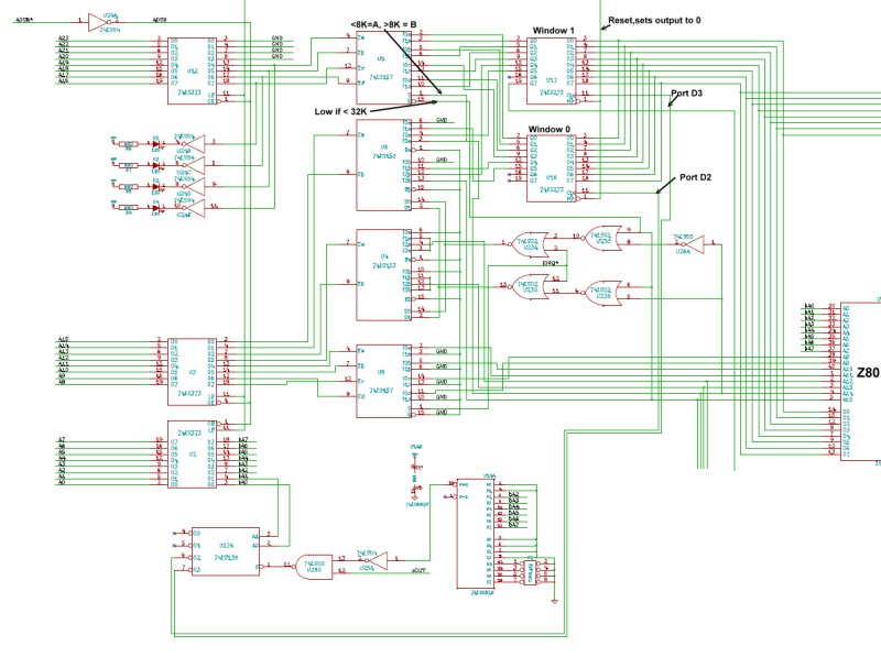
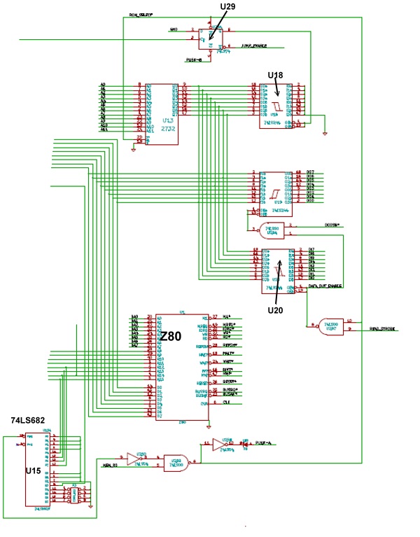
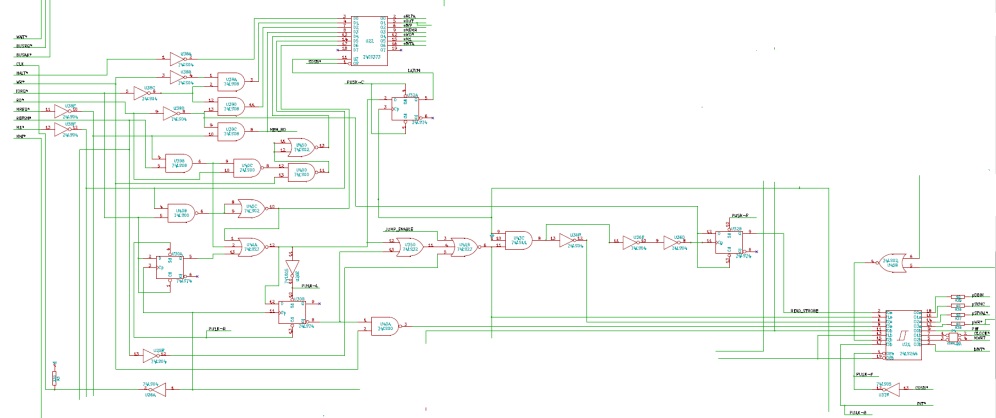
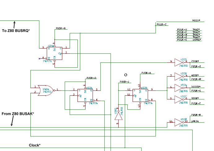
Here is a schematic of the third Z80 Prototype board. The board layout can be seen here

The board in my bus actually "works most of the time"  at 11 MHz However it's not completely reliable at these speeds.  Some day I may try tweaking the above chips some more.  At 10MHz it's completely reliable. It works fine too handing control over to an 8086 as a master/slave switch. It also appears to work fine with the interrupts from the PIC/RTC board.

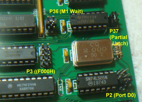
Here is a picture of the Final Z80 Master CPU Board.
Final Z80 Board

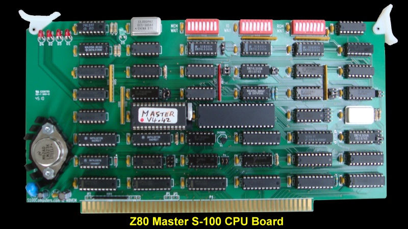
Two very small errors exist on the board - resistor R41 is a carry over from a previous version. It is connected to nothing. Ignore it. Also C1 should be something like a 47uF Tantalum cap (25V) rather than a 0.33uF as shown on the board silkscreen.  Also note the large 3A voltage regulator is close to the right hand side of the board. I found it neceassary to clip off two of the "fins" so the card would easily slide into my card cage.  I think the square type heat sinks would be OK.

Unlike many of the other boards on this site you cannot build and check out the board in stages. To start with however use a 2 or 4 MHz clock oscillator.  If your board does not come up at these speeds, change your Monitor code in EPROM to one with an EPROM with just 76H's (HALT) and see if you can get the Z80 
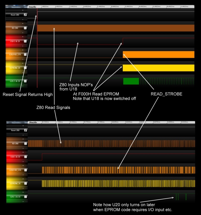
to always halt after a reset. If it does not, check the POC circuitry and see above how the board steps through memory addresses to arrive at the boot EPROM 
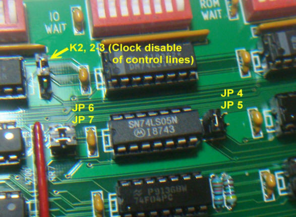
address.  If you are using our SMB none of the jumpers JP4-7 need be used.  Of course you can disable them on the SMB and use them here if you like.  Lastly don't expect this board to run at 10MHz speeds in a non-terminated S-100 bus or with old/slow S-100 memory boards.

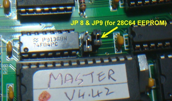
Note if you decide to use a EEPROM such as a Samsung MK28C64A 8KX8, you have to place it at an 8 K boundary. So in high RAM this would be at E000H.  If you want to use E000H-FFFFH for your monitor then that's fine. More typically however you will need only 4K for a monitor starting at say F000H to FFFFH.  In this situation you can either program the second 4K of the EEPROM's 8K space and  jumper JP8 1-2  and P39 5-6 (i.e. utilize A1 and A12) and set the POJ jumper P3, to F000H, or alternatively just program the lower 4K of the EEPROM's 8K space and force the EEPROMS A12 line to low, so jumper JP8 10-2 as before, but jumper P39  3-4.   BTW, you can have a second completely different second monitor in the EEPROM switchable to the upper or lower half of the EEPROM with jumpers P39 3-4 or 1-2. 
You must also be sure to "burn" your monitor into the upper or lower half of the EEPROM. (For the upper half, using a Wellon VP-280 Programmer, the "Load Buffer Address" would be 1000H, the "File Address" is F000H).

Hopefully this is not too confusing.  If so, start with an old 2732 EPROM and burn your initial monitor in that chip.
 
For a 10 MHz system with the 74Fxx or 74Sxx  chips I mentioned above, here are pictures of the jumpers to get you going.

  Jumper s1 Jumpers 2
     
  Jumper 3 Jumpers 4

  
A Production S-100 Board.
Realizing that a number of people might want to utilize a board like this together with Andrew Lynch at N8VEM (see here) we have completed a run of these boards. We will collect names for a second batch if needed.  If you have an interest in such a bare board, let Andrew  know via e-mail at:-  lynchaj@yahoo.com
 
Please note all the above clearly applies only to people who know what they are doing and can  do a little soldering and board assembly.  There will be little hand holding at this stage.

The links below will contain the most recent schematic of this board.
Note, it may change over time and some IC part or pin numbers may not correlate exactly with the text in the article above.

MOST CURRENT Z80 CPU BOARD SCHEMATIC  (V2, FINAL, 02/28/2010)
MOST CURRENT Z80 CPU  BOARD LAYOUT  (V2, FINAL, 02/28/2010)


Other pages describing my S-100 hardware and software.
Please click here to continue...

This page was last modified on 09/16/2011